Capstone Project for the Master of Engineering Program, University of California, Berkeley
August, 2016 – May, 2017
Title: Improving Reliability of 3D Printed Materials in Biomedical Applications
- Worked on the corrosion aspects of metal additively manufactured parts, in the context of orthopedic implants.
- Performed mechanical testing in corrosive environments to understand how such characteristics change with changes in surface characteristics and other factors, as a result of the additive manufacturing process.
- Examined failure surface using standard metallographic techniques
- Used this data to generate design guidelines for additively manufactured implants
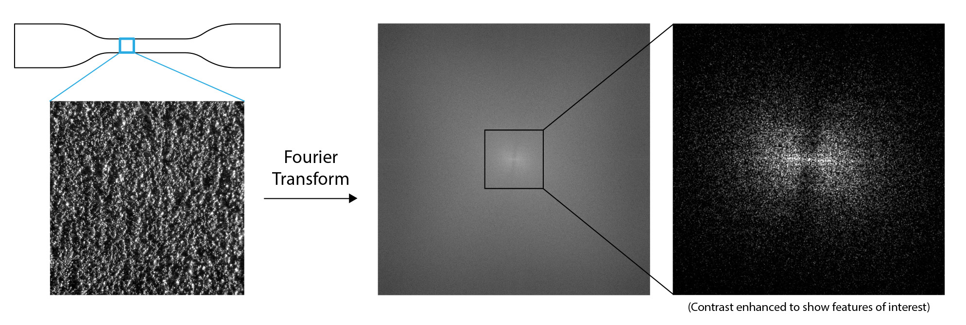
A Fast Fourier Transform (FFT) of a micrograph from the surface of an additively manufactured part is shown here. Anisotropy can be easily detected using this technique.
Fourier transforms can be used to conveniently detect anisotropy in micrographs. This technique is useful for micrographs of the surface, and also of the internal microstructure. While anisotropy is expected is many additive manufacturing processes, it is not always possible to detect the direction of anisotropy.
This technique can also be applied to check how the anisotropy in microstructure has changed once the additively manufactured part has undergone a post-procesing step, such as a solutionizing heat treatment.
Image: Own work
Bachelor's Thesis at Direct Digital Manufacturing Laboratory, Georgia Tech, Atlanta
May – December, 2015
Title: Quantitative Metallography Aided Experimental Characterization and Design-of-Experiment Based Process Optimization for Single-Crystal CMSX-4® Ni-base Superalloy Processed Through Scanning Laser Epitaxy (SLE)
Project guide: Prof. Suman Das (Professor & Morris M. Bryan, Jr. Chair in Advanced Manufacturing Systems, George W. Woodruff School of Mechanical Engineering, Georgia Institute of Technology)
- Learned about additive manufacturing technologies that can be used for metals in general, and for non-weldable alloys such as Ni-based superalloys in particular. This particular process can add immense value to customers in the commercial aviation industry by enabling remanufacturing of high-value parts, such as hot-section turbine blades, thus dramatically extending end-of-life of these parts and providing substantial savings.
- Gained insight into the process control required for obtaining fully dense deposits that are metallurgically bonded to the substrate.
- Understood the conditions that favour epitaxial growth of crystals, and how they can be utilized for obtaining deposits that are microstructurally continuous with the underlying substrate.
- Performed experiments as a part of a Design-of-Experiment based process optimization for the single crystal Ni-based superalloy CMSX-4, to determine the best processing parameters for different geometries.
- The experiments are followed by sectioning of the sample and metallography. The obtained micrographs are processed using a quantitative metallography image processing code, developed exclusively for this process.
- The final goal is to be able to develop a function that is able to predict the processing parameters for any given geometry, such that a deposit with a good single crystal height can be obtained.
- The idea of this particular single layer high-thickness process is to be able to obtain a fully dense, metallurgically bonded, microstructurally continuous deposit over hot-section parts whose life is limited by wear, such as the tip of a turbine blade. Once such a deposit is obtained, it can be machined to the the required precise geometry and put back to service, for a fraction of the cost of a newly cast part.
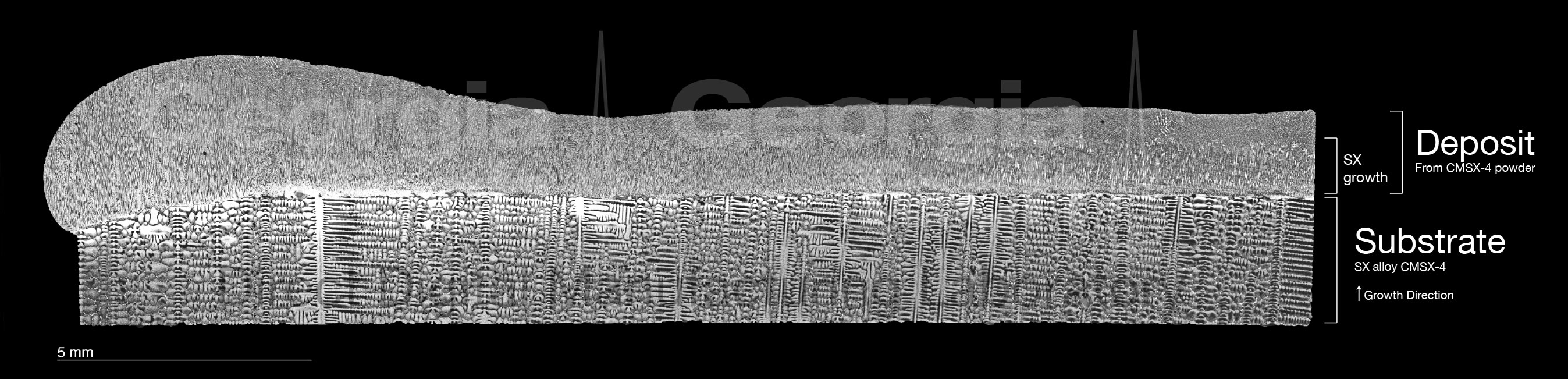
Representative lengthwise cross section of a CMSX-4® sample with the starting edge on the left side of the image. The substrate is a single crystal slab, cast with the marked growth direction. This simulates the tip of a turbine blade, where epitaxial addition of material as demonstrated here can be used to repair the worn out tip.
This particular sample is from experiments conducted by me, for my Bachelor's Thesis. More information is available from the lab's official website, here.
Image: Own work
Summer internship at Manufacturing and Materials Technologies, GE Global Research, Bangalore
May – July, 2014
Title: Investigation of recrystallization due to compression straining in Ni-based superalloy GTD 444.
Internship Supervisor: Dr. Sachin Nalawade
Manager: Dr. Sanjay Sondhi
- Experienced the scale at a large multi-national corporation that manufactures many different products, from light bulbs to jet engines.
- Experienced the workflow at an Industrial R&D lab for the first time. The internship was at the John F Welch Technology Center, GE's Largest R&D campus in the world.
- Learned about Ni-based superalloys, with particular attention to Single Crystal (SX) and Directionally Solidified (DS) superalloys that find application in Last Stage Buckets (LSBs).
- Gained exposure to the scale of operations in the field of Gas Turbines and comprehended the importance of the smallest positive change in properties with regard to efficiency and market dynamics.
- Understood the importance of microstructure, and how subtle changes therein could result in large changes in macroscopic properties.
- Undertook an observational study of Solution Heat Treatments (SHT) and gained insight into its criticality.
- Performed systematic metallographic analysis on the heat-treated samples in an effort to find recrystallized grains. The investigation was performed under the optical microscope, although the SEM was also used occasionally.
- Analyzed and quantified micrographs using image processing techniques.
- Due to the terms of the non-disclosure agreement, the project report may only be provided on request. Please send me an email if you would like to read it.
- An assessment from the mentor is available here.
Summer project at Department of Materials Engineering, IISc, Bangalore
May – July, 2013
Title: Investigation of Liquid Electromigration in Gallium
Project guide: Prof. Praveen Kumar (Department of Materials Science and Engineering, IISc, Bangalore)
- Studied flow pattern formation due to electromigration and thermomigration (in Gallium).
- Worked in the National Nanofabrication Facility at the Centre for Nano Science and Engineering, IISc (CeNSE, cense.iisc.ac.in).
- Learned to use a Micro System Analyzer, an instrument used to visualize surface topography.
- Gained experience with image and video processing techniques, and mathematical analysis tools.
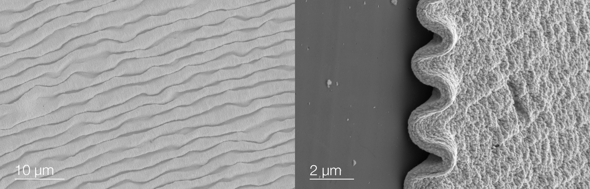
Electron micrographs of the flow pattern obtained.
Left: Surface morphology of the flow region shows the periodic pattern obtained.
Right: The morphology at the edge. The gallium film, as well as the underlying substrate are both visible. This micrograph was obtained by performing SEM on a tilted sample.
The nominal spacing is about 2 µm. Future work is expected to be focused on using this process to manufacture diffraction gratings.
(Commercially available gratings for visible light nominally have 500 lines/mm, or one every 2 µm)
Image: Own work